Huawei Signals Major Breakthrough in Semiconductor Technology
- May 28
- 2 min read
Huawei has announced an entirely new direction in semiconductor development that operates independently of advanced Extreme Ultraviolet (EUV) lithography machinery.
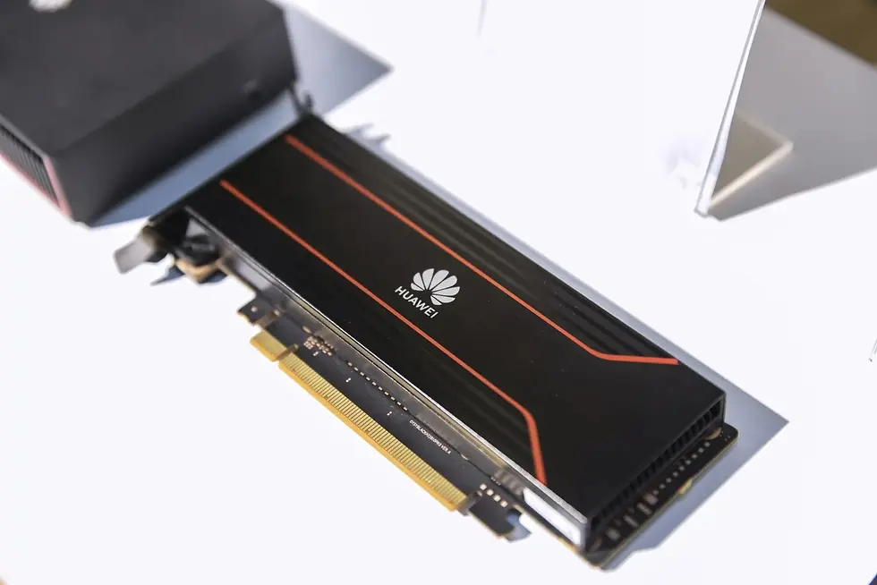
Huawei announces new direction for chip development and production
At a press conference on May 25, He Tingbo, President of Huawei's Science Advisory Committee and head of its semiconductor division, presented the Tau ($\tau$) Scaling Law. Huawei describes this new principle as a framework guiding "the co-evolution of both semiconductors and electronic systems."
Building on this law, Huawei concurrently unveiled its "LogicFolding" architecture. This technology is designed to reduce resistance and capacitance during signal transmission, thereby increasing transistor density without requiring upgrades to lithography equipment. The company aims to achieve a transistor density equivalent to a 1.4 nm process node by 2031.
This target represents the absolute vanguard of global semiconductor technology, aligning with the roadmaps currently pursued by industry giants TSMC and Samsung through multi-billion-dollar investments in next-generation EUV systems.
The crux of Huawei’s announcement lies in He's assertion that lithography advancements are "no longer essential" under the company’s new trajectory. The strategy takes direct aim at the single largest bottleneck currently facing the Chinese semiconductor industry.
Under U.S. sanctions, Chinese firms are prohibited from purchasing EUV machines from the Netherlands-based sole manufacturer, ASML. Theoretically, this restriction blocks them from manufacturing chips at the 3 nm node or below using conventional methods. If the LogicFolding architecture performs as claimed, Huawei will have successfully engineered a workaround to bypass this geopolitical barrier.
This is not the first time Huawei has caught the industry off guard with its semiconductor capabilities. In 2023, the company debuted the Mate 60 Pro featuring the 7 nm Kirin 9000S processor. The breakthrough stunned Western analysts, who had widely believed that tightening trade restrictions would prevent China from achieving such a milestone.
However, a massive chasm remains between a theoretical breakthrough and commercial mass production. Demonstrating a 1.4 nm-equivalent transistor density on paper is one matter; executing high-volume manufacturing with acceptable yield rates is an entirely different challenge. It is an obstacle that even market leaders TSMC and Samsung routinely spend years solving with each new technology generation.
Nevertheless, Huawei’s announcement sends a clear signal. It underscores that rather than waiting for international sanctions to ease, China is aggressively forging an independent path forward for its domestic semiconductor ecosystem.


Comments